Language:


What is a HDI PCB?
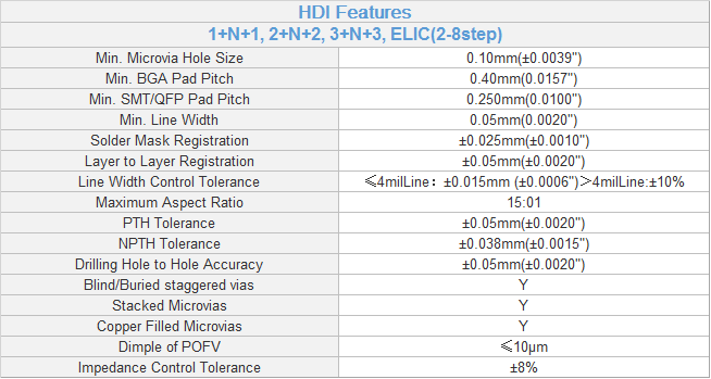
IPC-2226 defines HDI as a printed circuit board with a higher wiring density per unit area than conventional printed circuit boards (PCB). They have finer lines and spaces ≤ 100 µm / 0.10mm, smaller vias (<150 µm) and capture pads <400 µm / 0.40mm, and higher connection pad density (>20 pads/cm2) than employed in conventional PCB technology.
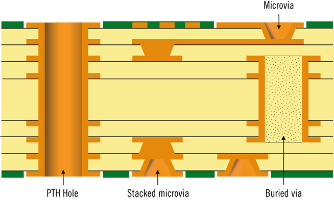
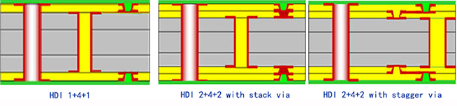
In 2010, PCGL Electronics improved its manufacturing facilities by HDI boards manufacturing to our comprehensive capabilities in PCB Fabrication and PCB Assembly. Comparing to Conventional Rigid PCB, HDI PCB request much higher wiring density with finer trace and spacing, smaller vias and higher connection pad density. Blind and buried vias'design is one of their marked feature. Currently the advanced HDI technology we used include: "Copper Filled" for special stack microvia, "Laser Direct Imaging"(LDI) is specifically designed for fine line technology, to eliminate dimensional stability problem of artwork caused by environmental and material issues. "Direct Laser Drill"(DLD) is drilling of copper layer by direct CO2 laser irradiation, compare to additional laser drilling with conformal mask, the copper direct laser drilling is capable of providing higher accuracy, better hole quality and better efficiency for HDI projects.
High Density Interconnects (HDI) are utilized to meet the market demand for complex designs in smaller form factors across the majority of market segments including Wireless, Telecom, Military, Medical, Semiconductor and Instrumentation. HDIs overcome the limitations found in standard circuit technologies through the utilization of ultra-thin cores, fine line processing and alternative via methods to reduce the size and weight of your components.
Contact: Mr. Michael Zou
Phone: +8615989475697
Tel: +86-755-27678837
Email: mc@pcgl-electronics.com
Add: 206, Huichuang2018 Creative Industrial Park, Gushu1st Road, Bao’ an District, Shenzhen City, China.