Language:


With the rapid development of Artificial Intelligence (AI), Edge Computing has become a crucial part of AI system architecture. Deploying AI algorithms at the edge not only significantly reduces latency and bandwidth usage but also enhances data security and real-time responsiveness. At the core of this advancement lies a high-performance, compact, and reliable Printed Circuit Board (PCB).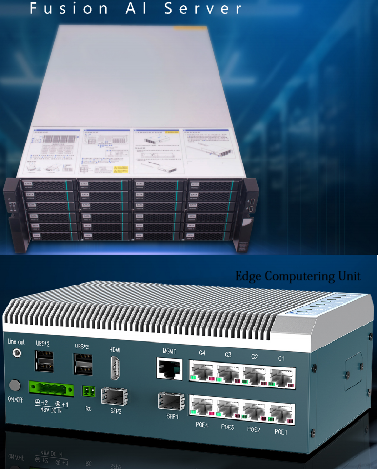
AI edge devices are often deployed in environments such as industrial automation sites, smart surveillance systems, autonomous vehicles, and edge servers. These scenarios impose stringent requirements on PCB design and manufacturing:
High Layer Count: To integrate high-speed processors, AI accelerators (e.g., NPU/TPU), high-capacity memory, and multiple I/O interfaces, boards often require 12, 16, or even 24+ layers.
High-Speed Signal Integrity: Communication through PCIe, DDR4/DDR5, USB 3.0/3.2, MIPI, and other high-speed protocols demands strict impedance control, layer stackup design, and EMC optimization.
High Power Density and Thermal Management: AI inference chips generate significant heat. PCB design must support effective heat dissipation using thick copper layers, thermal vias, and heat-conductive materials.
EMI/EMC Control: AI edge systems require careful layout, grounding, and shielding to ensure electromagnetic compatibility, particularly in high-frequency and wireless scenarios.
The PCB is the backbone of signal transmission. Whether it's PCIe links between AI accelerators and main processors, or MIPI CSI lanes to camera modules, the layout and routing quality on the PCB directly influence system performance and reliability.
AI chips demand multiple high-current, low-noise power rails. A well-designed PDN with power/ground planes and decoupling capacitors ensures voltage stability and minimal ripple under dynamic loads.
As part of the thermal path, the PCB helps dissipate heat through thicker copper, large ground areas, thermal vias, and thermal interface materials (TIMs). Mechanically, the board must also maintain structural integrity in harsh operating environments.
With growing demand for compact and integrated designs, PCBs are evolving into platforms for System-in-Package (SiP) or modular designs, where SoC, memory, power management, and I/O components are densely packed into a single high-density PCB for edge AI modules.
We have supported numerous clients with high-performance PCB solutions for edge AI applications, including:
AI Edge Gateway Motherboards (24-layer HDI boards)
Featuring Qualcomm, NVIDIA Orin, or Intel Movidius processors with 5G, dual Ethernet, camera interfaces, and industrial I/O.
Autonomous Driving Controller Boards (20-layer high-Tg boards)
Designed for L2/L3 autonomous driving, supporting CAN-FD, automotive Ethernet, LVDS, and GNSS communication modules.
Industrial Vision Processing Modules (12-layer boards)
With high-speed image processors, MIPI interfaces, and multiple AI accelerators for machine vision tasks.
We utilize premium materials to meet the demanding needs of edge AI applications:
High Tg FR4 (e.g., Shengyi S1000H / ITEQ IT180A) for thermal stability
Low-loss high-speed materials (e.g., MEGTRON 6, Rogers) for >10Gbps signal support
Reliable surface finishes (ENEPIG, ENIG, OSP) for multiple reflow cycles and long-term reliability
Our manufacturing capabilities include:
Up to 32-layer stackups
Laser-drilled blind and buried vias, HDI, any-layer interconnect
±10% impedance control
Rigorous quality control with flying probe testing, AOI, X-ray, and CNC inspection
Contact: Mr. Michael Zou
Phone: +8615989475697
Tel: +86-755-27678837
Email: mc@pcgl-electronics.com
Add: 206, Huichuang2018 Creative Industrial Park, Gushu1st Road, Bao’ an District, Shenzhen City, China.